How to Solve Obstacles in Mini LED Displays: An Introduction to Mass Transfer
From:Dongguan HCP Technology Co.,LtdTime:2023-01-01
In recent years, the development of Micro/Mini LED displays has been in full swing. After several years of cultivation and precipitation, Micro/Mini LED display has gradually made key breakthroughs and frequently come into the public's view. According to industry specifications, a Mini LED display refers to LED devices with chip size between 50-200μm, while a Micro LED display refers to a chip size of less than 100μm.
Mini LED display is a continuous improvement version of the backlight device, while Micro LED display is the future industry development target. And both of them gain public recognition with their high brightness, high refresh rate, energy saving, and other distinctive advantages.
According to statistics, the global Mini LED display market reached around $150 million in 2021 and is expected to exceed $ 2.32 billion in 2024 with rapid growth. Although the future growth scale of the Mini LED display market is promising, Mini LED displays still face one obstacle: how to transfer the chip quickly and perfectly. Therefore, how to solve this obstacle has become the key for LED display manufacturers wanting to gain a foothold in the Mini LED display market.
2 Problems with Chip Transferring Technology
The following are the main technical bottlenecks faced by many Mini LED display manufacturers.
The Chip Is too Small to Transfer
Traditional chip transfer technology and the equipment to transfer chips have certain physical limitations. For instance, Mini LED chips need to be bigger for conventional equipment to transfer efficiently, not to mention to meet the future demand for Micro LED microchips.
Low Transfer Efficiency
Conventional chip transfer equipment usually takes a long time in order to be able to complete the transfer of small chips, which in turn leads to low transfer efficiency, high costs, low yield rate, and cannot meet the needs of batch production.
HCP: Mini LED Display Leader You Should Know
To realize the demand for mass production brought by the commercialization of Mini LED display and to lay a good foundation for the popularization of Micro LED display, solving the above two technical problems is the key to success. With in-depth research of market demand, deep plowing of the underlying technology, and focus on innovation and practice, HCP has independently developed the patent: mass transfer technology.
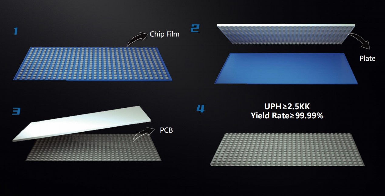
Mass transfer technology is the process of correctly and efficiently moving millions or even tens of millions of micron-sized LED dice onto a circuit substrate through an innovative technology after the fabrication of the Mini LED micron-sized dice is completed. Our patented mass transfer technology not only overcomes the challenge of doubling the pixel density but also solves the problem of difficult-to-meet yield rate.
3 Advantages of HCP Mass Transfer Technology
Our mass transfer technology effectively addresses industry pains for the following reasons.
1. Significant Improvement in Yield Rate
In terms of the difficulty of the mass transfer technology, how to increase the yield rate is the key. For example, the yield rate of our Mini LED display can reach 99.9999%, which means there can only be one defective chip for every million chips transferred, and the accuracy of each chip must be controlled within ±0.5μm.
2. Significantly Increase the Speed of Transfer
We adopt laser transfer technology to automate the mass transfer technology. Therefore, with the help of full-line automated production, we can place millions of micron chips on PCBs fast and accurately, achieving UPH ≥ 2.5KK/hr.
3. 100% Yield after Repair
HCP mass transfer technology not only solves the market bottleneck but also locates bad spots and detects them precisely. For example, our inspection equipment maps out R/G/B coordinate gears by determining the chip brightness and threshold value after lighting up. After automatically and precisely identifying and locating the bad spot, our fully automated technology will re-grab the spot to fix the chip, as well as infrared laser welding, to achieve the repair. Finally, it is worth mentioning that our technology can achieve a 100% yield rate after repair.
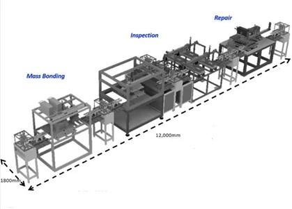
HCP mass transfer technology can achieve high speed, high quality, and high consistency transfer efficiency, realizing more than 30 times of traditional transfer speed, effectively solving the production bottleneck of the Mini LED display industry. In the future, we will continue to deepen our efforts in LED display technology and transfer technology and strive to become a key player in the LED display industry to help commercialize the use of COB LED displays and Mini LED displays.
Recommend



 No. 17, Sangyuan Industrial Road,Dongcheng District, Dongguan City,Guangdong Province, China, 523000
 +86 769 86738999
 info@hcpled.com

